
- SoC Solution
-
RTL Design, Platform Design & Verification, FPGA Verification 부터
Design Service 분야의 DFT Insertion, Layout, PKG / Test까지
시스템반도체 개발 및 제작에 필요한 모든 솔루션을 제공합니다.
Design Service Flow
-
STEP 1
Spec. Decision
RTL Coding -
STEP 2
Synthesis
-
STEP 3
Netlist
Hand-off -
STEP 4
DFT
-
STEP 5
Placement
Routing -
STEP 6
Verification
& PG -
STEP 7
Test Vector
Generation -
STEP 8
Failure
Analysis
Design Service Level
| Level |
Spec. Decision |
Synthesis |
DFT |
Placement |
Verification |
Test Vector |
Failure |
|---|---|---|---|---|---|---|---|
|
Level 0
Spec. Hand-off |
|||||||
|
Level 1
RTL Hand-off |
|||||||
|
Level 2
Netlist Hand-off |
|||||||
|
Level 3
GDS Hand-off |
Total Solution
-
FULL CHIP DESIGN
( SPEC / DESIGN )Design / Verification Platform
System Architecture Analysis
Power Management Control
Real Emulation with FPGA
IP Supplier Partnership
Device Driver, BSP, OS porting
-
PHYSICAL
( SYNTHESIS / DFT )
IMPLEMENTATIONDFT (SCAN / BIST / JTAG)
In-system Test
STA (Static Timing Analysis)
Synthesis & Timing Closure
-
PHYSICAL DESIGN
( AUTO P&R )Full Chip Floor Plan
Hierarchical Physical Design
Low Power Design
SI Check
(IR Drop, Crosstalk-Noise) -
PKG & TEST Develop
( Assembly & TEST )Package Design
Test vector generation
ATE test set-up
Qualification & Reliability
Q.A & Failure analysis
-
Mass Production
( SCM )Wafer Business
Full Turn-key Business
(Wafer + PKG + TEST)
Advanced Technology
-

- AI / HPC
- AI Accelerator, Datacenter, Server, Cloud Computing, Edge AI, XR/AR Processor
-

- Automotive
- ADAS, Digital Cockpit, Network Processor, Vision Processor, Automotive MCU
-

- Consumer
- High-Performance MCU, Printer SoC, Smart home, AI SoC for Wearables, AI Edge Processor
-

- Industrial
- Security SoC, AI ISP, Smart Mobility, Industrial Robot, Digital Twin
Vision & Mission

-
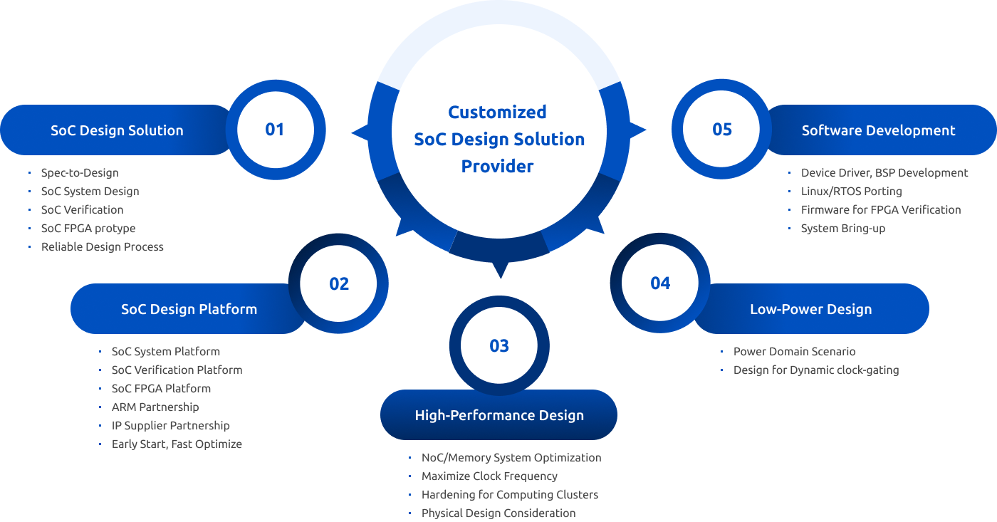
01
SoC Design Solution
-
Spec-to-Design
SoC System Design
SoC Verification
SoC FPGA protype
Reliable Design Process
-
02
SoC Design Platform
-
SoC System Platform
SoC Verification Platform
SoC FPGA Platform
ARM Partnership
IP Supplier Partnership
Early Start, Fast Optimize
-
03
High-Performance Design
-
NoC/Memory System Optimization
Maximize Clock Frequency
Hardening for Computing Clusters
Physical Design Consideration
-
04
Low-Power Design
-
Power Domain Scenario
Design for Dynamic clock-gating
-
05
Software Development
-
Device Driver, BSP Development
Linux/RTOS Porting
Firmware for FPGA Verification
System Bring-up
SoC Design Solution
-
01
SoC DesignSoC/System Architecture
Processing Core
IP/xPU Hardening
Full Chip TOP Integration
PPA Optimization
-
02
SoC VerificationIP/System Verification
FPGA Prototyping
Emulation for Architecture
SoC TOP Verification
Sub Platform Verification
-
03
Software SolutionSoC Architecture Software Stack
BSP (Board Support Package) to SDK (S/W Development Kit) TF-A (Trusted F/W), OP-TEE (Trusted OS), U-Boot, RTOS (Zephyr), Linux (Device Driver/Tree), Buildroot
System Solution Optimization
Performance Optimization
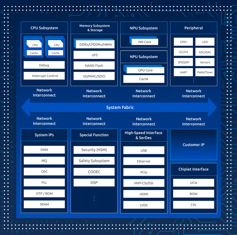
- SoC System Platform
- Arm Based SoC System: Ready from Entry level to Cutting Edge
- 3rd Party IP through Partnership
- Early Access and Fast Optimization
- SoC Verification Platform
- Systematic Configured & Re-usable Environment
- All Verification Cases from Top to Sub in One Environment
- Configurable Alternative Models for Integrated Units
- Light and Reliable against Integration Issue
- Easy Porting your System into One Verification Env.
- SoC Design Solution
- FPGA board with SoC System Platform
- Fast Emulation for your IP on SoC System Platform
- Fast Emulation for your System
- Fast Iteration for your IP / System Architecture
Physical
Implementation
-
Hardening for
Computing Clusters -
CPU
GPU
NPU
Hash Core
-
Physical & Power-aware
Logic Synthesis -
Logic Synthesis with physical information and power scenario
Placement-Aware Multi-Bit Register Banking
Physically aware Clock Gating restructuring
Design for Testability
-
Support advanced
DFT solutions -
Low pin count test with serializer
Power Aware DFT
Test Fail Diagnosis
-
Memory BIST
(Built-In Self Test) -
Memory BIST/BIRA for higher SRAM yield
Repair solution with eFuse & OTP
-
Logic BIST
-
hardware based in-field testing method
on-chip generated random patterns for safety and mission critical applications
-
In-system test
-
for safety-critical applications such as automotive, aerospace, and medicine
Use IST(In-System Test) controller through IJTAG network
to access the chip during operation
-
SCAN
(Advanced DFT Skill) -
Scan test for improved test coverage for lower DPPM
Stuck-At, Bridge, Transition, Path-delay, OCCT, Burn-in
-
IDDQ Test
-
IDDQ test for additional fault coverage
-
Boundary Scan
-
Inter-chip connection test method for system level testing
-
Physical DFT consider
-
Physical Reordering and Repartitioning
Physical Design
-
Accurate and
robust timing analysis -
LVF based variability library
Moment-based LVF to cope with non-Gaussian effect
Parametric OCV method
CCS/CCSN-based STA
Statistical Rvia STA
NP-Skewed corner STA for hold timing, min-pulse, and DCD check only
-
Physical optimization
-
BEOL-aware delay optimization (BEOL resistance increase impacting path delay)
Mixed DDB/MDB Flow
-
Physical-aware Timing ECO
-
Minimize physical side-effect for ECO
-
MIM-aware Timing ECO
-
Produce a single ECO file for Multiply Instantiated Module
Accelerate multi-core CPU/GPU timing closure
-
01
Dynamic Power OptimizationMulti-supply Voltage & Voltage Island
In-Rush Current prevented power gating
Clock/Memory-Gating
Dynamic Voltage Frequency Scaling
Vector-Driven Optimization
Decap pre-placement method
Merge or split ICG / Multi-bit flip-flop
Low Power CTS (Concurrent Clock and
Data Optimization) -
02
Leakage Power OptimizationMulti-Vth Optimization
Gate-Length Biasing
Sign-off Leakage Optimization
-
03
Low Power VerificationLow power static rule check
Power-aware Simulation
Power-aware equivalence check
-
01
Power Integrity SolutionPower Plan based on Early Prototyping Analysis
Dynamic Voltage Drop Analysis
Static Power Analysis
Power EM / BUMP Current
P/G Resistance check
-
02
Signal Integrity SolutionSignal EM
Glitch Noise analysis
Clock Jitter validation
Duty-cycle distortion methodology
Clock Propagation Check
3-row decap inverter on CTS